Knowledge Articles

Revealing Crystal Defects with Low-Dose SED and HPT‑100 Plasma Cleaning
Defects inside molecular crystals called dislocations can affect how materials perform in electronics, pharmaceuticals, or coatings. Until now, imaging these defects has been hard because the microscopes needed too much electron energy, which damages fragile organic crystals.

Delivering genetic material such as RNA or DNA into human cells is a central challenge in the development of next-generation medicines - from gene therapy to RNA-based vaccines. In the search for safer, more stable delivery platforms, researchers are increasingly turning to polymer brushes: nanoscale coatings made of densely packed, hair-like polymer chains tethered to a surface.

2D materials, are crystalline solids consisting of a single layer of atoms. These materials have unique properties due to their thickness being limited in one dimension, which makes them ideal for various applications including optoelectronics, energy generation, and high-performance composites. As an example, the most widely studied 2D material, graphene, has exceptional conductivity and is stronger than steel.

A recent preprint published on bioRxiv explores the structural organisation and selective packaging mechanisms of the influenza A virus genome using a high-throughput DNA-PAINT approach. Researchers at the University of Oxford and the University of Warwick analysed more than 10,000 individual virus particles, gaining insights into how influenza genome segments interact and assemble during viral replication.
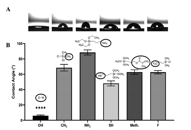
A recent study from Loughborough University demonstrates the impact of organosilane surface modifications on cardiovascular implants. The research focuses on modifying surfaces with various silane groups such as amine, methyl, and thiol to selectively enhance endothelial cell growth while suppressing smooth muscle cell proliferation. This dual effect helps address two critical issues in cardiovascular implants: improving endothelialization and preventing thrombosis.
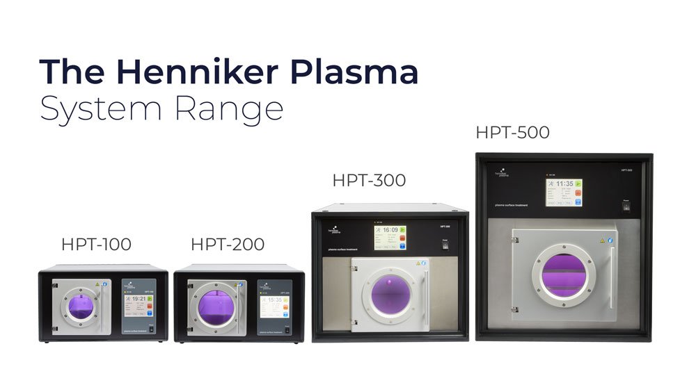
For a limited time only, Henniker Plasma is offering incredible upgrades when you purchase from our range of HPT plasma systems. Take advantage of these exclusive offers, valid until the end of 2024!

Recent advancements in memristor technology highlight the potential of monolayer graphene electrodes in electronic devices. A recent study has successfully demonstrated the fabrication of a memristor featuring a monolayer graphene electrode directly deposited onto sapphire substrates using a commercially available metal-organic chemical vapour deposition (MOCVD) system. The incorporation of the Henniker HPT-100 plasma system in the fabrication process allows for batch production, accommodating up to 37 wafers simultaneously, showcasing a scalable approach to device manufacturing.
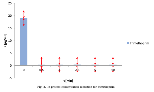
The promising results of pharmaceutical removal from water using atmospheric plasma.
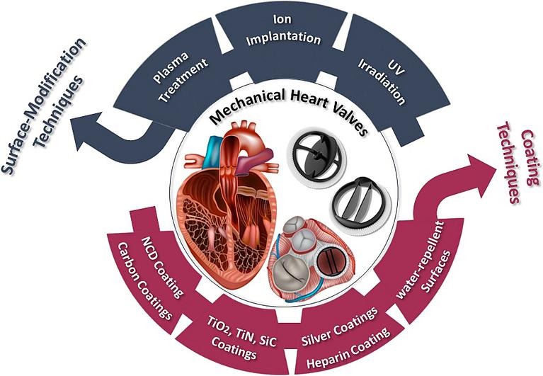
Advancing Biomedical Engineering Through Innovative Surface Modifications
Addressing the PFAS Challenge with Plasma Surface Modification
PFAS (Per- and polyfluoroalkyl substances) are widely known for their exceptional water- and grease-resistant properties. However, their environmental persistence and potential health risks have sparked a significant movement towards finding safer alternatives. PFAS-free polymers have emerged as a promising solution, but achieving the desired surface properties without these chemicals has been a challenge.