Plasma surface etching is a type of plasma treatment used to increase the surface area of a material on the microscopic scale. The surface of the component is etched with a reactive process gas.
Material from the surface is etched away, converted to the gas phase and removed by the vacuum system. The surface area is greatly increased, raising the surface energy and making the material easily wettable. Plasma surface etching is used before printing, gluing and painting and is particularly useful for processing of e.g. POM and PTFE, which cannot otherwise be printed on or bonded without the use of aggressive chemicals.
Plasma surface etching effects
 Untreated surface
 Plasma treated surface
 Plasma Etching Explained
Plasma Etching Explained.
The final video in our series on plasma treatment technology, this video explains how plasma surface etching works.
Controlled Reactive ion etching
Reactive ion etching delivers a highly directional flux of energetic, reactive ions to the material surface. In doing so, a precisely controlled patterning of the substrate occurs as an un-masked sample is etched away by the reactive ions. Each of our plasma systems can optionally be fitted with a reactive ion etch electrode making them a perfect, low-cost laboratory development tool in applications such as semiconductor or organic electronics research.
 Before Plasma Treatment
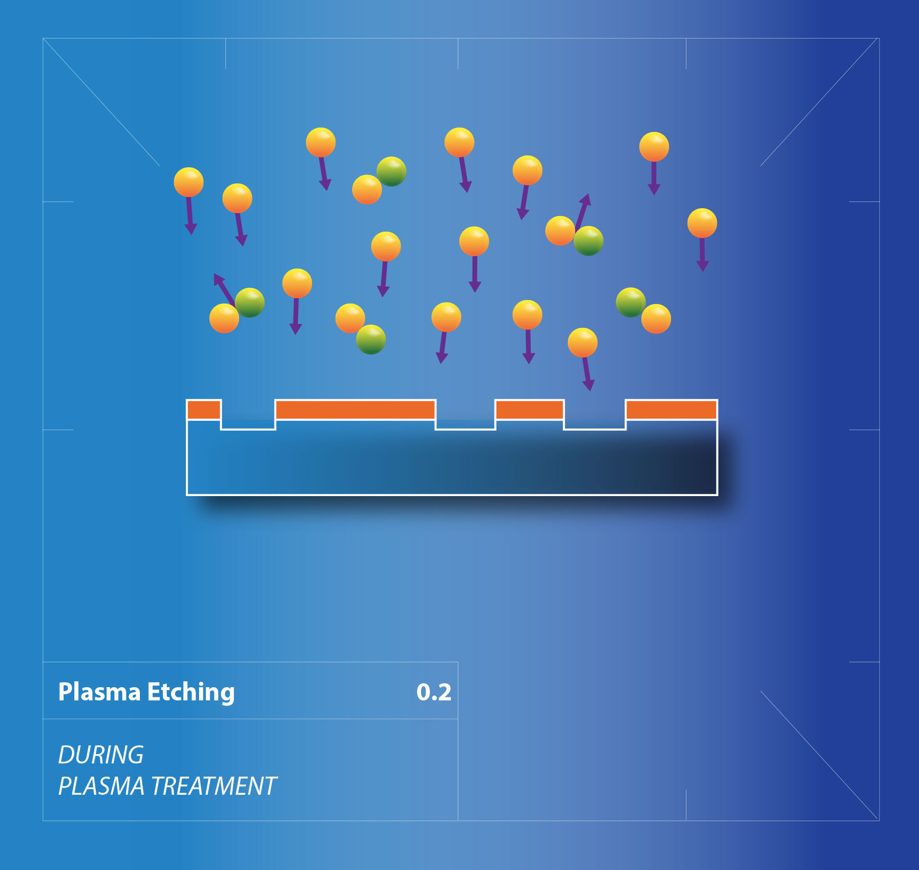 During plasma treatment
  After plasma treatment
Plasma etching is suitable for e.g.:
- POM, PTFE, FEP, PFA
- PTFE compounds
- structuring silicon
- photoresist ashing