Thin-Film Layers for Fast Diagnostics
![]()
Functional thin film layers, such as those that can be manufactured using plasma deposition techniques, are central in many microelectronics technologies. Microvisk are developing these techniques in the production of new diagnostic devices for point of care blood clotting test devices, the extremely hydrophilic surface of the sensor ensuring that even when using a tiny drop of blood, the viscosity can be accurately defined.

Microvisk Ltd., the British life science company, use their two diagnostic devices CoagMax and CoagLite determine the degree of blood coagulation, an area in which they have pioneered a completely new approach. Whilst similar handheld devices in the quickly growing industry use optical analysis or chemical reactions, Microvisk devices use a disposable test strip with miniaturized chips based on Micro Electro Mechanical (MEMS) technology to measure blood viscosity.

MEMS devices combine solid state electronic and mechanical operating elements manufactured on a nano-scale on a silicon wafer. The key advantages of MEMS structures compared to conventional electro-mechanical systems are their high reliability, small power consumption, reduced dimensions and low cost.
Microvisk uses these advantages to monitor the degree of blood coagulation in their unique, patented handheld MEMS-based systems, by means of the so-called prothrombin test which they have now brought to the market.
The devices are currently undergoing clinical testing in Germany and the United States. The device lends itself to simple patient self-testing, with a disposable test strip, the Smartstrip. Experts predict that there is high commercial potential given that there are estimated to be some seven million people in the Western world who take the anticoagulant Warfarin, and within this demographic a large number will be used to using diabetes self-test devices. The Food and Drug Administration (FDA) estimates that every year one million new patients are added to this list.
Patients requiring regular blood tests often had to have the procedure carried out by a doctor.
“Intial self test devices which were released onto the market proved fragile and too complicated to be used at home”
says John Curtis, CEO of Microvisk.
“They also needed large amounts of blood.”
Blood on the Microlitre Scale
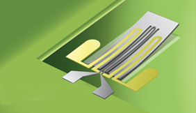
Only a tiny drop of blood is needed when using Microvisk devices, a microlitre scale amount is taken from the fingertip, and viscosity is then determined using a highly flexible micro-cantilever device which is made of silicon.
This 3D-structure interacts with the tiny amount of blood used in the test, moving up and down in response to the sweeping and dumping of the medium. This motion generates a tiny electrical signal which can be analysed to give an accurate measure of the blood viscosity. Blood clotting and viscosity changes go hand in hand with the coagulation process and can be identified using a single physical process monitor.
Conditions for reliably measuring results require that the tiny amount of blood sufficiently wets the surface of the microcantilever. Since this surface normally repels liquid, the challenge facing them was to create a permanently hydrophilic surface. Microvisk considered various solutions and began trials with us following consultations about thin-film plasma polymerization.

“With plasma polymerization, it is possible to create a thin surface that is permanently hydrophilic without affecting the function of the MEMS”,
says Bob Ibbotson, sensor development scientist,
“with a wet chemical process such thin layers are not possible.”
Our Solution
Nanoscale layers - Using our low-pressure plasma polymerisation systems, nanoscale, well-controlled polymer layers are deposited at the Microvisk production facility in North Wales. Using this procedure, a very low contact angle can be achieved and these results are stable and visible for long periods after testing.
Hydrophilic surfaces have been produced for many years with plasma technology, but the durability of these layers has usually had a limited lifetime. However, keeping within the appropriate parameters of the process we succeeded to produce a permanent solution, working hand in hand with the Microvisk team to develop the exact coating process that they required.
Plasma polymerization is a widely used method for the deposition of thin films at low pressure. The coating process can produce both isolated inorganic as well as continuous organic films with very functional characteristics - for example, optically transparent or self catalyzing. The thin, highly networked polymer layers can be generated with a wide range of properties on virtually any substrate.
Coating at fast speeds - In the coating process, monomers in a vacuum chamber are stimulated using a plasma, which is an ionized gas. The gaseous monomer is deposited onto any substrate that is immersed in the plasma where it forms highly crosslinked polymer layers. Microvisk process their MEMS sensors in a short cycle process at temperatures below 50 °C. The plasma is formed in a chamber by ‘igniting’ the gas/monomer mixture using a strong electric field between the substrate holder, which serves as an electrode, and an additional counter electrode. Polymerized reactive particles are created on the silicon surface by the electrical discharge. The molecules of the original material must have double bonds, triple bonds or ring structures and therefore chain-forming atoms such as carbon, silicon and sulphur are favoured.
“The coating process is effective and reliable. It guarantees high coating rates at relatively low operating costs to us”
, says Microvisk CEO Curtis.
“This reflects and assists our philosophy to bring a diagnostic tool to the mass market. In addition to the use of MEMS, the plasma surface treatment is a fundamental building block.”
Ecological aspects were an additional reason for Microsvisk’s decision in favour of plasma polymerization. Due to increasing environmental requirements, many conventional wet-chemical coatings must be replaced with “cleaner” processes with a lower environmental impact.
This example shows that new application areas for microsystems technology can be developed through new layer technologies via close co-operation with our clients. In modern materials research and development, the functionality of a surface is becoming a critical area in which organisations can add significant technological and value-added benefits.